 Email
Email Print
Print


Semiconductor Photolithography Equipment Market - Forecast(2025 - 2031)
Semiconductor Photolithography Equipment Market Overview
Semiconductor Photolithography Equipment Market Size is forecast to reach $11685.1 Million by 2030, at a CAGR of 9.5% during forecast period 2024-2030.This growth is primarily attributed to the rapid development of the semiconductor industry, an increase in penetration of IoT and high demand for integrated circuits which are being installed in miniaturized electronic devices. Integrated Circuits are a key component in electronic devices and they are being produced through the immersion lithography technique in which a pattern from a photomask is crossed through a projection printing lens and then that photomask is transferred to the surface of the wafer by mask aligners instruments. Due to this growing demand for ICs, the Semiconductor Photolithography Equipment Market size is also on a rise. Additionally, due to technological advancements, innovative lithography processes such as e-beam lithography, EUV and immersion lithography are rapidly being adopted in the Semiconductor Photolithography Equipment market. These photolithography processes use cutting-edge mask aligners instruments and projection printing lenses to project a superior photomask pattern on the wafer surface. Such new innovations along with the increasing demand for semiconductors across all industry verticals are set to positively influence the Semiconductor Photolithography Equipment Industry Outlook.
Report Coverage
The report: “Semiconductor Photolithography Equipment Industry Outlook – Forecast (2024-2030)” by IndustryARC, covers an in-depth analysis of the following segments in the Semiconductor Photolithography Equipment industry.
Key Takeaways
- In the Semiconductor Photolithography Equipment market report, the EUV segment is analyzed to grow at a significant rate with a CAGR of 10.1% during the forecast period 2022-2027. This growth is due to the incorporation of AI, IoT and rapid technological advancements in the semiconductor lithography industry.
- Based on wavelength in the Semiconductor Photolithography Equipment Market report, the 70nm-1nm wavelength range is expected to grow at the highest rate of 10.4% during the forecast period. This growth is due to this wavelength range’s widespread applicability across various industry verticals and increased investment in the industry.
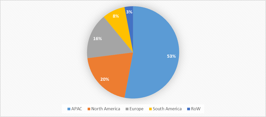
- APAC region had the largest share in the global Semiconductor Photolithography Equipment Market size with a share of 53%, owing to factors such availability of a number of high-voltage power stations, increased demand for power modules and the presence of major manufacturers.
Semiconductor Photolithography Equipment Market Segment Analysis - By Product Type
By Product Type, the EUV segment in the Semiconductor Photolithography Equipment Market report is estimated to grow with the highest CAGR of 10.1% during the forecast period 2022-2027. The incorporation of artificial intelligence (AI), growing usage of IoT devices and new technological advancements in the semiconductor industry, especially in projection printing lenses and mask aligners, are expected to drive demand for the EUV photolithography segment. Additionally, the increasing adoption of micro technologies including microprocessors and integrated chips, which are being produced by immersion lithography and other semiconductors, are also fuelling the market growth of the EUV segment in the Semiconductor Photolithography Equipment industry. In July 2022, in SEMICON WEST 2022, LAM Research Corp, Entegris and Galest INC announced a strategic collaboration that would provide semiconductor manufacturers worldwide with LAM’s dry photoresist technology for EUV lithography to produce next-gen semiconductors. This increased adoption is set to boost the EUV segment and thereby boost the Semiconductor Photolithography Equipment Market size.
Semiconductor Photolithography Equipment Market Segment Analysis - By Wavelength
Based on Wavelength, the 70nm-1nm segment in the Semiconductor Photolithography Equipment Market report is analyzed to grow at the highest CAGR of 10.4% during the forecast period 2022-2027. This growth can be attributed to this wavelength’s widespread applicability across various industry verticals, technological advancements and increased investment in the semiconductor industry. This wavelength is used in the production of NAND logic gates and DRAM (Dynamic random-access memory). It enables semiconductor manufacturers to produce low-cost memory chips. In October 2021, Samsung Electronics announced that it began mass production of 14nm Dynamic Random-Access Memory using 70nm-1nm wavelength range semiconductor devices. Due to this segment’s wide range of applications, the segment is facing significant growth. This is further influencing the Semiconductor Photolithography Equipment Market Industry.
Semiconductor Photolithography Equipment Market Segment Analysis - By Geography
APAC region dominated the global market for Semiconductor Photolithography Equipment Market with a market share of 53% in 2021 and is also expected to have significant growth over the forecasting period. The growth is driven by factors such as the availability of a number of high-voltage power stations, an increase in demand for power modules and an exponential increase in population. According to the Department of Electronics and Information Technology (DEITY), nearly 2,000 chips are designed in India each year, with over 20,000 engineers working on various aspects of chip design and verification. Additionally, the presence of major manufacturers boosts the Semiconductor Photolithography Equipment market growth in the APAC region.
Semiconductor Photolithography Equipment Market Drivers
Rapid growth in electronic device use and technological advancements in the semiconductor industry:
The expansion of the consumer electronics devices sector throughout the world, increasing demand for photolithography in the manufacturing of printed circuit boards & microprocessors and rapidly increasing semiconductor industry are the major factors driving the Semiconductor Photolithography Equipment Market. Photolithography technology has numerous advantages, including high light sensitivity, excellent adhesion properties, high resolution and the ability to 3D encapsulate cells inside hydrogels. All of these are propelling the market forward. For instance, in October 2021, Nikon announced the launch of FX-6AS, a new photolithography system, which can be used for manufacturing OLED and LCD panels for latest electronic devices such as smartphones, laptops and others. These new technological advancements are set to drive the Semiconductor Photolithography Equipment Market size.
Increasing demand for Integrated Circuits in developing nations and the Presence of major manufacturers:
The constantly rising demand for electronic devices is boosting the demand for integrated circuits as well. Especially in developing regions such as Taiwan (China), the demand for integrated circuits is so high because the majority of the manufacturers of integrated chips are based in these regions and these circuits are a key component in making electronic devices. This rising demand in these regions drives the growth of the Semiconductor Photolithography Equipment Industry. In July 2020, Taiwan Semiconductor Manufacturing Co. (TSMC) announced that around 50% of all semiconductor photolithography equipment that are being installed and operational worldwide are supplied by TSMC. This huge presence of major players is poised to change the Semiconductor Photolithography Equipment Industry outlook positively.
Semiconductor Photolithography Equipment Market Challenge:
The constantly changing Semiconductor Industry and high cost of Semiconductor Photolithography Equipment:
The high installation and maintenance costs associated with Semiconductor Photolithography Equipment act as a major obstacle to market growth. The constantly changing semiconductor industry also acts as a restraint to the Semiconductor Photolithography Equipment Market growth. For instance, ASML's most advanced machines, known as EUV lithography systems, cost around US$150 million each. This high cost associated with the systems eventually leads to expensive end products, which further hampers the Semiconductor Photolithography Equipment Market growth.
Semiconductor Photolithography Equipment Industry Outlook
Product launches, collaborations, and R&D activities are key strategies adopted by players in the Semiconductor Photolithography Equipment Market. The top 10 companies in the Semiconductor Photolithography Equipment industry are:
- ASML
- Canon
- Nikon
- Veeco Instrument
- LAM Research Corp
- Samsung Electronics
- Carl Zeiss AG
- Taiwan Semiconductor Manufacturing Company Limited
- Shanghai Micro Electronics Equipment Ltd
- JEOL Ltd
Recent Developments
- In July 2020, Canon Inc. introduced FPA-8000iW, the first Canon semiconductor photolithography system. It is primarily used to support the manufacturing of large panels, which are common in back-end processing. This launch has eventually helped the company increase its market share.
- In January 2021, LAM research corp. introduced Vantex, which can provide improved performance and more extendibility for current and next-gen NAND and DRAM memory devices made out of Semiconductor Photolithography Equipment. This is poised to increase the company’s market share in Semiconductor Photolithography Equipment Market.
- In Jan 2022, ASML and Intel Corporation announced the renewal of the latest phase of their longstanding collaboration to improve semiconductor photolithography technology. This collaboration is set to increase the Semiconductor Photolithography Equipment Market size.
Key Market Players:
The Top 5 companies in the Semiconductor Photolithography Equipment Market are:
- ASML
- Canon Inc.
- Nikon
- Veeco Instruments Inc.
- Carl Zeiss AG
For more Electronics Market reports, please click here